

Message from Professor Sekitani
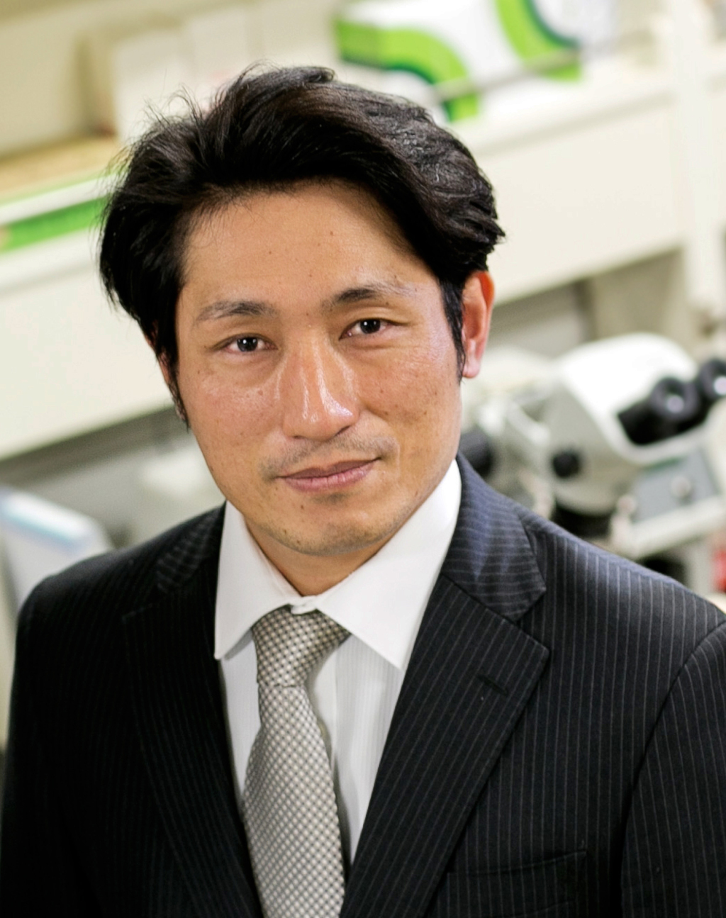
Our days as an undergraduate or graduate student are very valuable and the experience obtained during this period will be a great asset to you. I hope you will tackle many challenges during these days. If you have questions or want to visit our laboratory, contact Tsuyoshi Sekitani
(sekitani(atmark)sanken.osaka-u.ac.jp).
Sekitani Lab. is affiliated with【The Department of Applied Physics, Graduate School of Enginnering, The University of Osaka】. If you are interested in joining Sekitani Lab., please refer the following WEB.
http://www.ap.eng.osaka-u.ac.jp/graduate/en/
If you have questions, please contact Tsuyoshi Sekitani
(sekitani(atmark)sanken.osaka-u.ac.jp).
We will welcome your visit.
Achievements
Conferences
(keynote)
Conferences
(invited)
News & Information

For Students who wish to go to Sekitani Lab.
The motto of our laboratory is to develop advanced technology based on fundamental science. On the basis of this motto, the laboratory aims to nurtureindividuals with a wide range of knowledge who have theability to promote and lead innovation in multidisciplinary fields ranging from physics, chemistry, and electronics to biotechnology. In addition, we aim to cultivate energetic students who constantly engage their hands and brains, have the patience to learn through trial and error, and continuously strive to improve. This is our ideal student model.
Sekitani Laboratory belongs to the Department of Precision Science & Technology and Applied Physics, Graduate School of Engineering, The University of Osaka, within the Applied Physics Course.
If you are interested in applying, please visit the department’s official website.
Graduate School of Engineering, The University of Osaka
Department of Precision Science & Technology and Applied Physics, Applied Physics Course
For information about orientation sessions, please check the links below:
Course Website: http://www.ap.eng.osaka-u.ac.jp/graduate/
Facebook: https://www.facebook.com/oubutsu/
If you have any questions, please feel free to contact Prof. Sekitani (sekitani(atmark)sanken.osaka-u.ac.jp).
We look forward to welcoming you to our laboratory.
*Please replace “(atmark)” with “@” when sending your email.
Career paths of alumni (examples)
University of Cambridge, Shimadzu Corporation, SECOM, DENSO, Tokyo Electron, The University of Tokyo, Toray Industries, Panasonic Information Systems, ROHM, etc. (in alphabetical order)
Access
Sekitani Lab. SANKEN, The University of Osaka 8-1, Mihogaoka, Ibaraki, Osaka 567-0047 Japan
Tel: +81 -6-6879-8400
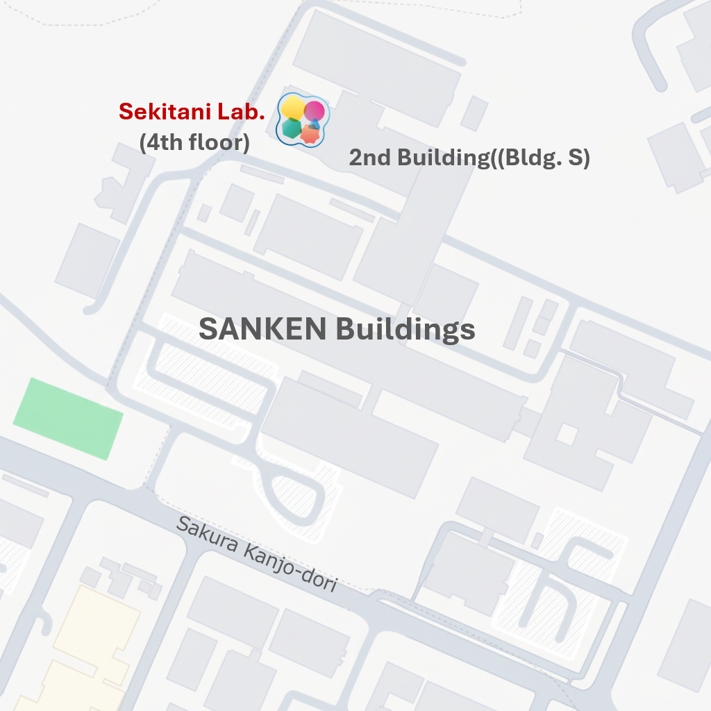
Sekitani Lab. is on the 4th floor of the SANKEN 2nd Building (Bldg. S).
SANKEN is located on the Suita Campus of The University of Osaka.