|
|
| Research on liquid crystal display |
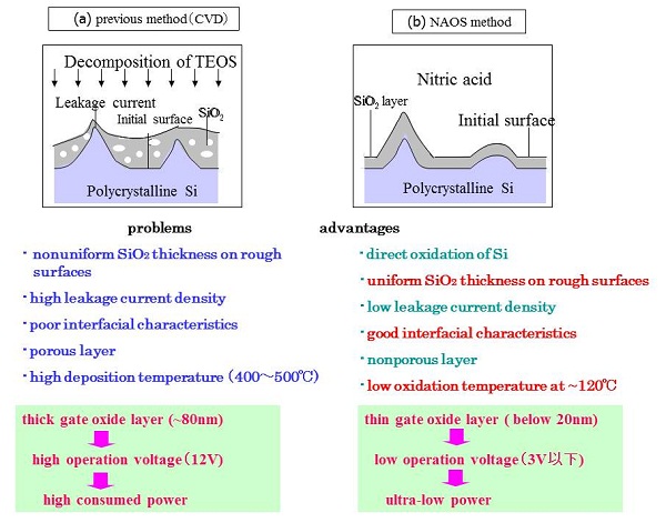
Figure 1 Formation methods of gate oxide in thin film transistors: (a) conventional
CVD method; (b) NAOS method developed in Kobayashi laboratory.
Liquid crystal
displays are driven by thin film transistors (TFT). TFT consists of metal-oxide-semiconductor
(MOS) structure, which is also the fundamental structure of LSI. Because LSI is fabricated on Si wafers, an
oxide layer on Si (i.e., gate oxide layer) can be formed by thermal oxidation
of Si, i.e., heating of Si at ~900°C in oxidizing atmosphere. On the other hand, TFT is fabricated on glass
substrates, and therefore an oxide layer should be fabricated below 500°C. For the low temperature formation of an oxide layer on Si, the chemical
vapor deposition (CVD) method is usually employed (cf. Figure 1a). However, using deposition methods, a uniform
thickness oxide layer cannot be formed especially on rough surfaces. A high density leakage current flows though
the thin oxide regions, and a thick oxide layer (e.g., 80 nm thick) is needed
to suppress the leakage current. The
thick gate oxide layer increases the operation voltage (i.e., 12 V for
commercial TFT), resulting in high power consumption since consumed power is
proportional to the square of the operation voltage. Moreover, Si surfaces before gate oxide
formation become interfaces after gate oxide deposition, leading to poor interfacial
characteristics due to contaminants present before deposition and incomplete
chemical bonds at the SiO2/Si interface. SiO2 formed by the deposition
method possesses a low density and contains unfavorable species such as water, resulting
in poor bulk properties.
In the case of nitric acid oxidation of Si
(NAOS) method, on the other hand, oxygen atoms and dissociated oxygen ions (O-) generated by decomposition of HNO3
directly react with Si, forming SiO2 (cf. Figure 1b). Therefore,
even on rough Si surfaces, a uniform thickness SiO2 layer can be
produced (Fig. 1b). The SiO2/Si
interface is formed in the place of Si bulk before oxidation, leading to good
interfacial characteristics. The atomic
density of the SiO2 layer is high, and the bulk properties are also
excellent. Consequently, the leakage
current density can be made low, which enables the use of a thin (e.g., 20 nm)
gate oxide layer. The thin gate oxide
layer makes it possible to operate TFT at a low voltage below 3 V, leading to a
vast decrease in power consumption.
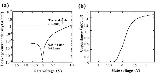
Figure 2 Electrical characteristics of the 1.3 nm SiO2 layer formed by the NAOS method at 120ºC: (a) current-voltage characteristics,; (b) capacitance-voltage characteristics.
Figure 2a
shows the leakage current density for the NAOS SiO2 layer formed on
crystalline Si by use of 68% HNO3 solutions. The leakage current density of the 1.3 nm
NAOS SiO2 layer is between 1/4 and 1/20 of that for a ~1.5 nm
thermal oxide layer formed at ~900°C.
This result indicates that application of the NAOS SiO2 layer
to TFT can greatly improve the electrical characteristics.
Figure 2b
shows the capacitance-voltage (C-V) characteristics of the NAOS SiO2/Si
structure. In the case of an ultrathin
oxide layer such as 1.3 nm thickness, measurements of C-V curves are of
difficulty because of a high density leakage current. However, the NAOS SiO2 layer has a
low leakage current density even when it is as thin as 1.3 nm, and
consequently, the C-V curve can be measured.
The observed C-V curve shows that the NAOS SiO2 layer
possesses excellent interfacial characteristics.
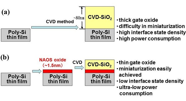
Figure 3 Gate oxide structures in TFT: (a) conventional TFT; (b) TFT with an ultrathin
NAOS oxide layer.
Figure 3a shows the conventional
structure of TFT, i.e., ~80 nm gate oxide layer on poly-Si or amorphous
Si. A ~1.5 nm NAOS SiO2 layer
can block a leakage current, and hence the thickness of a gate oxide layer
formed on the NAOS SiO2 layer can be greatly decreased (Figure 3b).
We have succeeded in fabrication of TFT with 10 nm gate oxide and the
operation voltage can be decreased to 1 V, resulting in a decrease of consumed
power to 1/144 of the conventional TFT operated at 12 V.
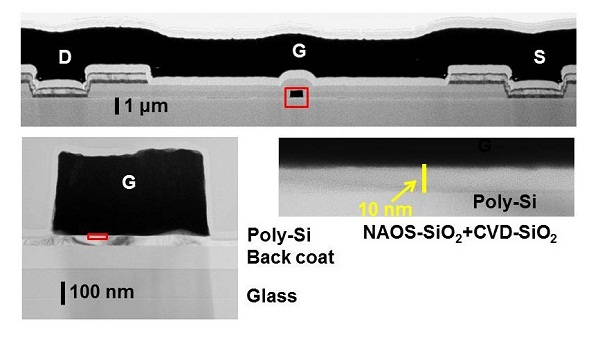
Figure 4 Cross-sectional transmission electron micrographs of the gate region in
TFT with the NAOS SiO2/CVD SiO2 stack gate structure.
Figure 4
shows the cross-sectional transmission electron micrograph (TEM) of TFT with a
NAOS gate oxide layer. The thickness of
the gate oxide layer is only 10 nm.
Between poly-Si substrate and a CVD SiO2 layer, the ~1.5 nm
NAOS SiO2 layer is present.
The NAOS SiO2 layer is observed with a darker color,
indicating a higher density than that that of the CVD SiO2
layer. This dense NAOS SiO2
layer can effectively suppress a leakage current.
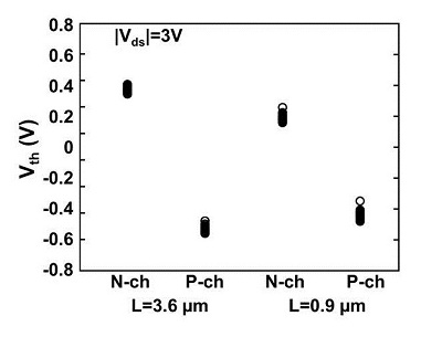
Figure 5 Threshold voltage of TFT with the NAOS SiO2/CVD SiO2 stack gate structure.
Figure 5
shows the threshold voltage of TFTs with the NAOS SiO2 layer (total
gate oxide thickness: 10 nm). The
absolute values of the threshold voltages for both N-ch and P-ch TFTs are less
than 0.5 V, which makes it possible to operate the TFTs at 1 V.
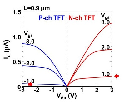
Figure 6 Drain current vs. the source-drain voltage for TFT with the NAOS SiO2/CVD SiO2 stack gate structure (total gate oxide thickness: 10 nm).
Figure 6
shows the drain current vs. the source-drain voltage for TFTs with the NAOS SiO2
layer (total gate oxide thickness: 10 nm).
The curves possess ideal saturation feature. Even at 1 V, the drain current is
sufficiently high, demonstrating that the TFTs can be operated at 1 V. The 1 V operation indicates that the TFT
power consumption is 1/144 of that of the conventional TFTs operated at 12 V.
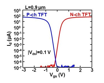
Figure 7 Drain current vs. the gate voltage for TFT with the NAOS SiO2/CVD SiO2 stack gate structure (total gate oxide thickness: 10 nm).
Figure 7
shows the drain current vs. the gate voltage for TFTs with the NAOS SiO2
layer (total gate oxide thickness: 10 nm).
The off-current is approximately 10-7 A, i.e., as low as the noise level,
indicating that the NAOS SiO2 layer effectively blocks the leakage
current. The curves possess steep
structure, showing good interfacial characteristics. The on/off ratio is 109, which is
approximately two orders of magnitude higher than those for conventional TFTs.
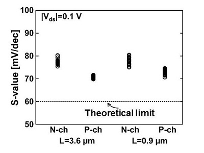
Figure 8 S values for TFT with the NAOS SiO2/CVD SiO2 stack gate structure.
Figure 8
shows the S-value for TFTs with the NAOS SiO2 layer (total gate
oxide thickness: 10 nm). S-value is
defined as an increase in the drain voltage to increase the drain current by
one order of magnitude. The S-value
decreases with a decrease in the gate oxide thickness and with the improvement
of interfacial characteristics. The
observed S-value is 70~80 mV/dec, which is close to the theoretical limit of 60
mV/dec, showing excellent interfacial characteristics of the NAOS oxide
layer.
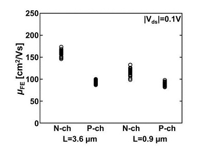
Figure 9 Channel mobility for TFT with the NAOS SiO2/CVD SiO2 stack gate structure (total gate oxide thickness: 10 nm).
Figure 9
shows the channel mobility of TFT with the NAOS SiO2 layer (total
gate oxide thickness: 10 nm). The
channel mobility for the N-ch TFT is 150 cm2/Vs, and that for the
P-ch TFT is 100 cm2/Vs. The
channel mobility does not depend on the gate length and the gate oxide
thickness. These results indicate that
the mobility depends only on poly-Si but not on the NAOS oxide layer. This demonstrates that due to excellent
interfacial characteristics of the NAOS oxide layer, it does not degrade the
mobility, and consequently the mobility is determined only by poly-Si
properties.
|
|
