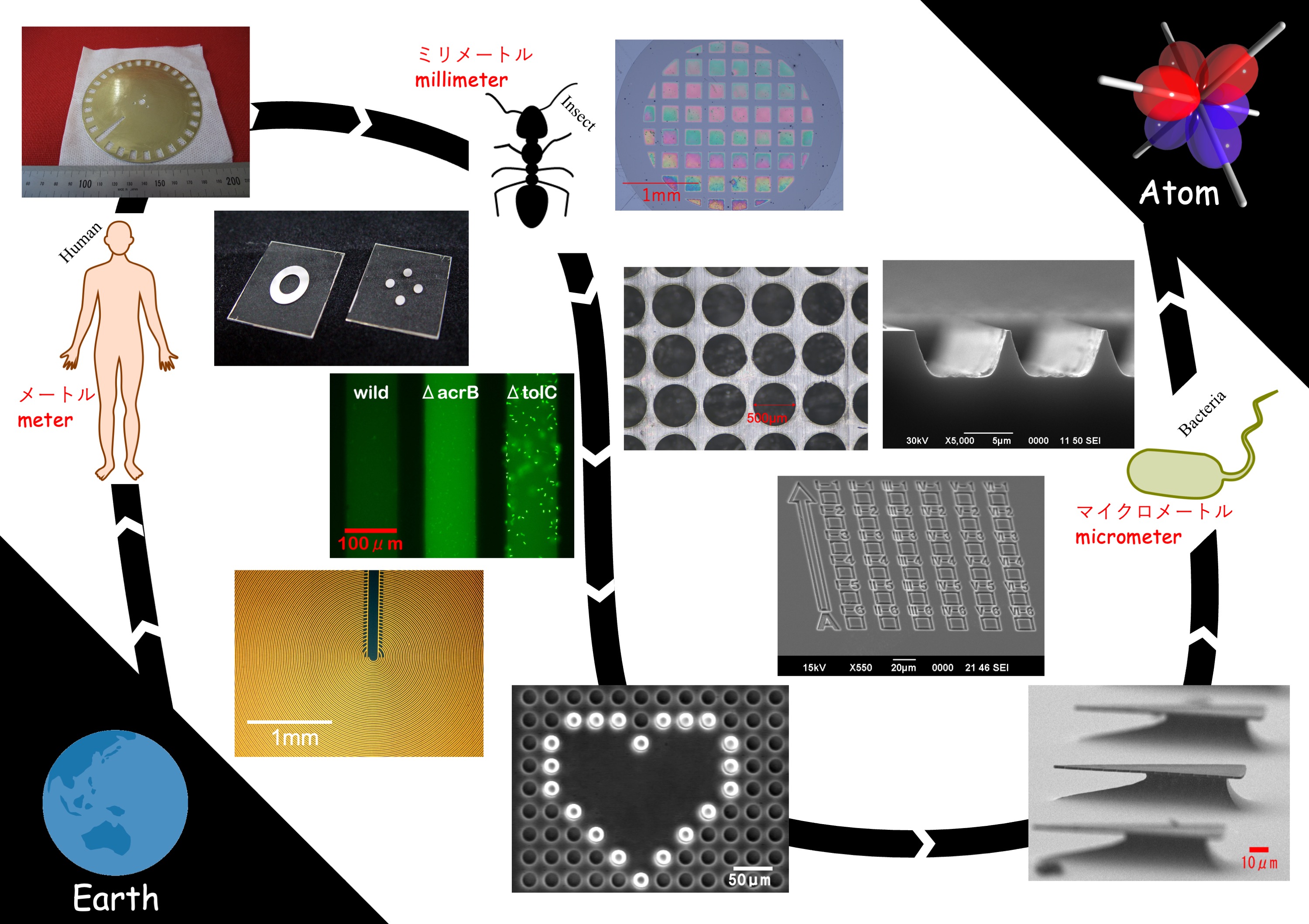
Equepment and Fee
| Name | External View | Description | Usage Fee (JPY/hour) |
|---|---|---|---|
| LED lithography (Maskless lithograpy) | 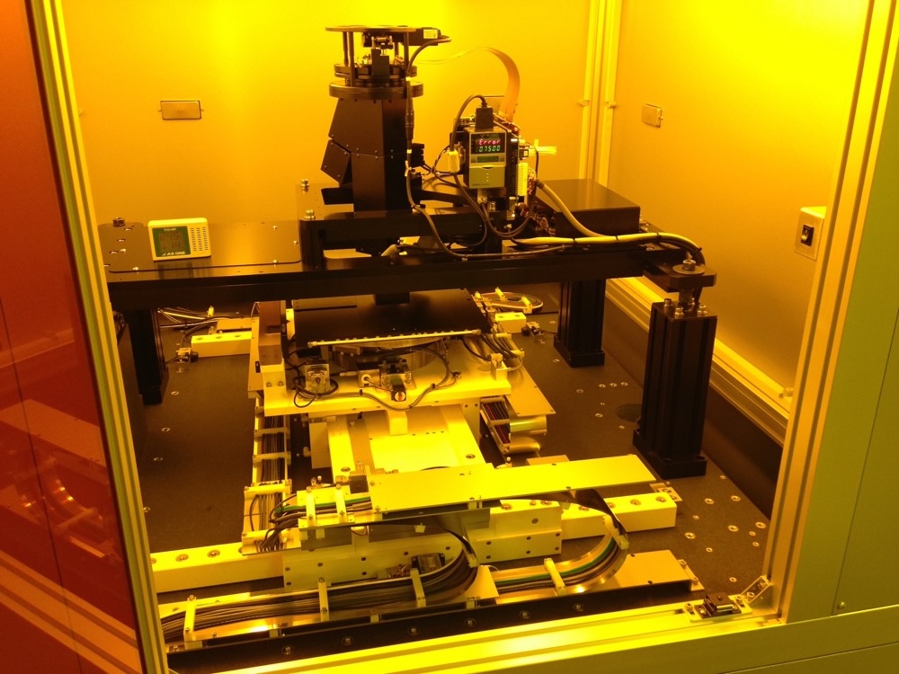 |
Exposure using a high-intensity 365 nm LED, Maximum patterning area: 100 mm × 100 mm, Minimum dot size: about 1 µm × 1 µm. |
1,000 | Mask Aligner | 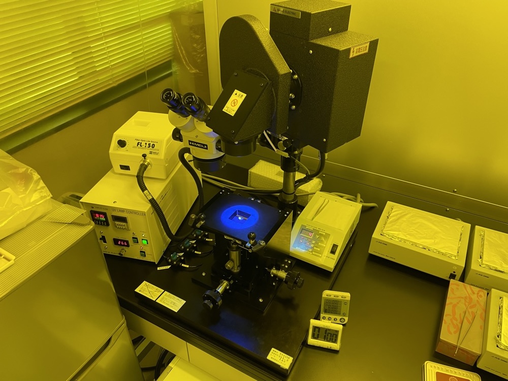 |
Mask window size: 4cm x 4cm. | 1,000 |
| Pulsed Laser Deposition | 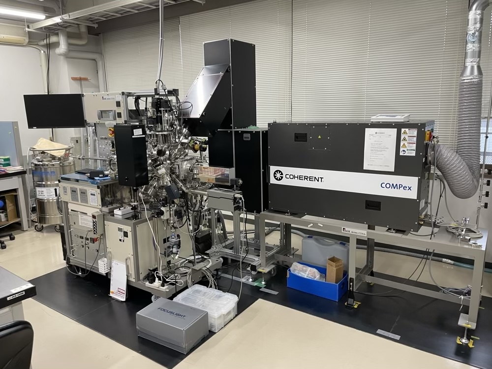 |
ArF laser (193nm), Oxigen Gas. | 12,000 |
| Reactive Ion Etching | 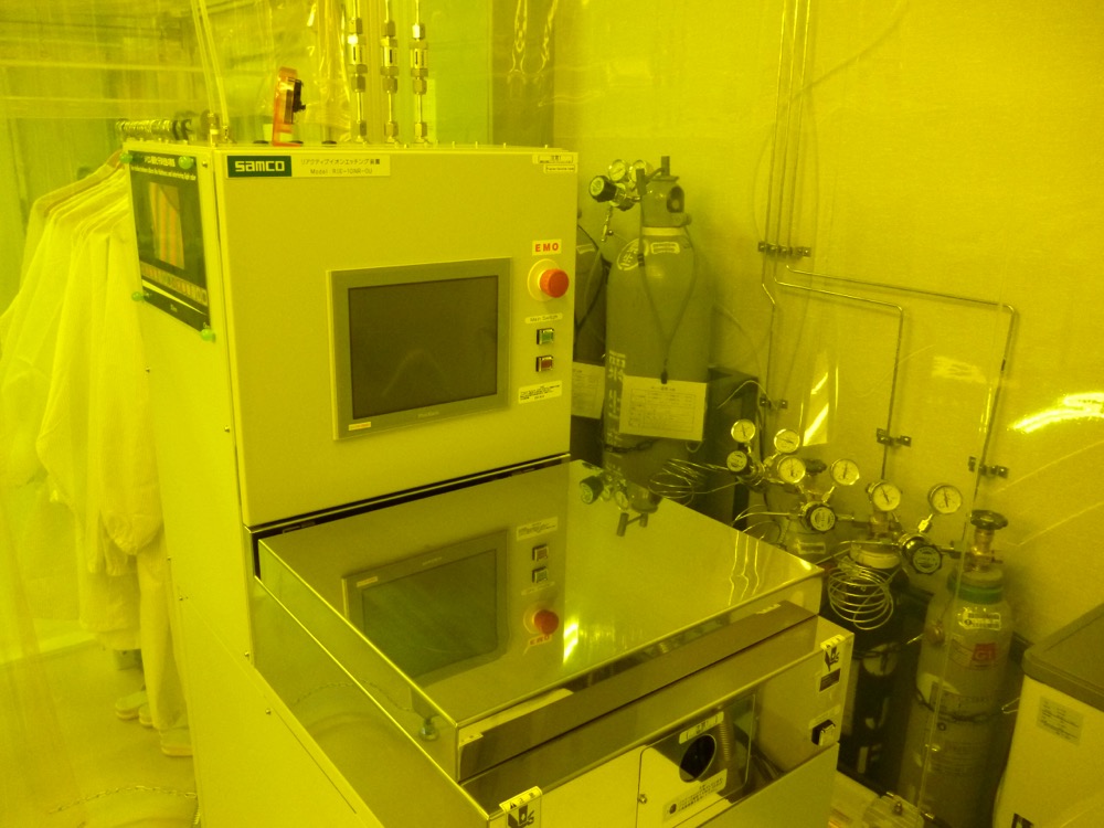 |
SF6, CHF3, and O2 gases are available. | 1,000 |
| Thermal evaporation system | 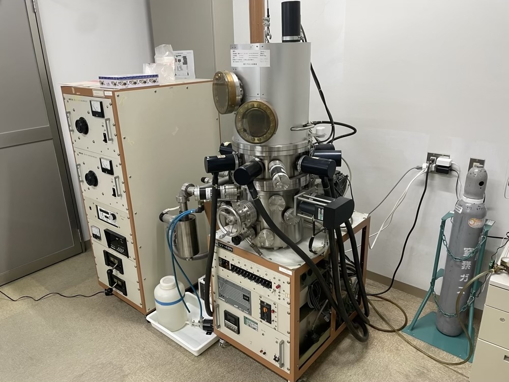 |
Metal films are deposited by resistive heating. | 1,000 |
- Technical assistance is provided, but LED lithography, Mask Aligner, and Pulsed Laser Deposition systems are also available for self-use.
- Fees are doubled for users from outside the institute, and tripled for companies engaged in joint research with the university.