Outline of research
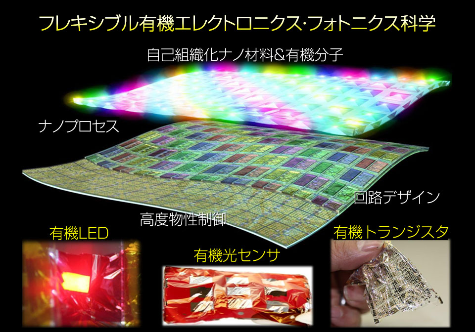
In our laboratory, we study science that fuses the basic science and advanced technologies required to precisely control the molecular structure, electronic state, and physical properties of various organic materials and to apply these technologies to realizing flexible electronics and photonics. The goals of our laboratory are to study various topics from theories based on basic science, including mathematics and physics, to systems that contribute to society.
When viewing the natural world, you may have been amazed at the diversity, unique functions, and profoundness of organic systems. Organic materials consist of carbon skeletons, which are the basic structures and have excellent properties and functions despite their relatively simple structure.
In our laboratory, we are studying and developing flexible electronic devices, organic electronics, and organic photonics utilizing the diversity and multifunctionality of organic materials. So far, we have studied and developed the world’s first large-area organic electronics, including
1) flexible organic flash memories utilizing the self-assembly of organic materials.
2) stretchable organic electroluminescence (EL) displays utilizing the flexibility of elastomers.
3) intelligent sheets that can transmit power and information.
4) braille displays equipped with a sheet-type polymer machine.
Along with the practical application of these electronics, we have, for the first time in the world, established measurement systems to clarify the electronic states and conduction mechanisms of flexible organic transistors. In addition, we have carried out leading research on physical property measurement; for example, we have clarified the mechanism of a unique conduction phenomenon of carriers observed when an organic circuit is bent and have succeeded in the world’s first measurement of the Hall effect of flexible transistors.
The basis of the development of these devices is basic science, such as quantum mechanics and solid-state physics. Students in our laboratory learn condensed matter physics and molecular chemistry in order to apply such basic science to real-life technologies.
Unique features of our laboratory
To design and develop new devices, a wide range of techniques and knowledge is required from the assessment of social needs, ideas for new devices, and the planning of technical strategies required to realize these ideas, to technologies for material synthesis, circuit design, fabrication processes, integration, systems engineering, and the evaluation of physical properties and characteristics, in addition to knowledge on electrical and electronic engineering. Students of our laboratory can be involved in every aspect of the above elements and acquire the skills required for the manufacturing of electronic devices.
Main research themes
- Organic devices using self-assembly phenomenon
- Many organic materials are accompanied by a self-assembly phenomenon, an important phenomenon not found in inorganic materials.
- Our laboratory aims to develop new thin-film devices by programming single molecules with a nanometer length using the self-assembly phenomenon and aligning them into a fine regular array.
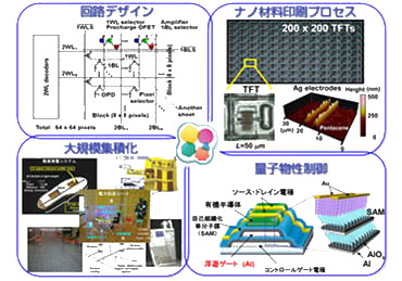
- Printing process, circuit design, and integration technologies of organic electronics
- Many organic materials can be printed on a large-area surface using ink jet printers because they dissolve in an organic solvent and various liquids. Only the required amount of material is printed on the required area of the surface; thus, the amount of material consumed is extremely small, enabling efficient processing. Therefore, printing technology is considered to be a very important process at the production sites of next-generation electronics.
- Our laboratory was the first in the world to apply ink-jet and screen-printing technologies to the fabrication of organic transistor integrated circuits, enabling us to realize large-scale printed electronics. We will further apply these technologies to the modeling of organic printed transistors, the development of new devices, and the exploration of new materials and phenomena.
- Exploration of new functions and development of new electronics using nanomaterials
- To realize user-friendly and flexible electronics, not only should the material itself be flexible but it should also have good electrical characteristics.
- Our laboratory has succeeded in developing a conductor that stretches like rubber and conducts electric current like a metal through the use of our original technology for uniformly dispersing carbon nanotubes in an elastomer. Using this material, we are developing new functional materials to realize new electronic devices and clarifying their physical properties.
- Furthermore, we aim to realize stretchable organic electronics that can cover any curved or movable surface by using new functional materials.
- Development of Flexible Sensors for Biometric and Low-Level Signal Measurement
- As population aging becomes a global challenge, gentle and flexible sensor devices that can unobtrusively interface with the human body are attracting increasing attention.
- Our laboratory develops sensor systems based on soft electronics, including organic device fabrication technologies and stretchable wiring techniques.
- In our sensor development, we integrate technologies such as low-power integrated circuit design, highly reliable communication system design, and advanced signal processing. Through this multidisciplinary approach, we strive to create devices that are truly practical and usable in real-world applications.