
Outline of research achievements
Our laboratory has been carrying out research on the physical properties of base materials used in flexible electronics and their applications on the basis of the excellent electrical and mechanical properties (e.g., flexibility), self-assembly phenomena, and low-energy processability of organic materials. In particular, we succeeded in realizing a high integration of organic transistors by developing technologies based on the characteristics of organic materials in a wide range of fields. These technologies include lamination technology for organic nanomolecular layers, technology to controlanorganic semiconductor/insulator interface, technology to control the physical properties of organic molecular materials, evaluation technology, and technology to design organic circuits. We established the fundamental technology for fabricating flexible organic thin-film transistors (TFTs) and developed ultraflexible electronics and stretchable electronics with excellent mechanical properties, demonstrating theusefulness of these devices for the first time in the world.
We have not only developed electronic devices, but also fabricated an 1) organic light-emitting diode (OLED) with a conjugated polymer or 2) organic photoelectric conversion element with a bulk heterojunction [solar cell, optical photodetector (OPD)] on a 1-μm-thick plastic film, realizing imperceptible electronics. This is expected to become the next-generation human interface and is being studied in cooperation with medical doctors to apply them to devices for use in next-generation medicine and medical welfare.
We have been developing new science fields ranging from information communication to medicine andmedical welfare using electronic devices, optical devices, and functional materialsthat consist of soft organic materials. In addition, we have demonstrated that these devices and materials can be used in new applications and have shown real examples of applications to society.
Our achievements have been presented through academic journal publications, invited talks, and presentations at international and domestic academic conferences.
For more details, please refer to the Publications page.
Major achievements
1 Improvement of performance of flexible organic transistors
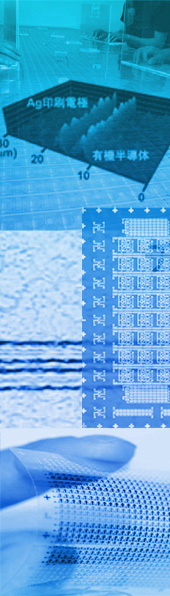
We established new technologies [e.g., lamination technology for organic nanomolecular layers, technology to control an organic semiconductor/insulator interface, technology to control the physical properties of organic molecular materials, and technology to design organic circuits (Nature Comm.2012, Nature Mater. 2010,2011, Science2009, Appl. Phys. Lett.2009, MRS Comm.2012)]to substantially improve the performance of organic transistors. In addition, we explored the field of flexible electronic devices fabricated using organic transistors before the rest of the world. In particular, we were the first to realize an ultraflexible organic transistor (bending radius,≤10 μm) thathasa high electrical performance (mobility of 3.2 cm2/Vs when driven at 2 V) exceeding that of amorphous siliconby combining various technologies related to materials, physical properties, processes, and circuit design in a concerted manner [Nature2013, Nature Mater.2010].
Thus far, high performances in terms of response speed (propagation delay time per stage, 22 μs; IEEE EDL2011), mobility at a low-voltage (3.2 cm2/Vs; Nature2013), mechanical flexibility (5 μmradius of curvature; Nature2013), heat resistance (250 oC;Adv. Mater.2013), and low noise (10−24 A2/Hz) were realized. We also established a fabrication process for organic transistors with the world’s highest performances in terms of the above-mentioned indices.
2 Evaluation and control of physical properties of flexible organic transistors
There have been no semiconductor devices with both high flexibility (bending radius≤1 μm) and excellent electric properties. In addition, the electron state and conduction mechanism of many semiconductor devices have not been clarified. We developed an original high-precision Hall measurement system to measure theminute Hall effect of organic transistors with a high impedance and succeeded in the Hall measurement of flexible organic transistors for the first time in the world (Appl. Phys. Lett.2006,2007). Using the system, wefoundthat the conduction mechanism in flexible polycrystalline organic transistors is different from that in high-mobility organic transistors with a single-crystal rubrene semiconductor layer. In the flexible organic transistors, carriers are transported by band conduction or hopping conduction involving thermal excitation as a result of controlling the molecular structures of organic semiconductors and the semiconductor/insulator interface. In addition, it was demonstrated that the conduction mechanismcan be controlled by selecting different materials for the channel interface.
In addition to the Hall measurement, we succeeded in the first precision measurement of flicker noise of organic transistors and found that the flicker noise is caused by the fluctuation of carrier densityowing to the presence of carrier traps. We realized the fabrication of flexible organic transistors with the world’s lowest noise level and only a small variation in theirproperties by minimizing the carrier trap effect as much as possible using technologies to control the semiconductor/insulator interface and thermal processing.
3 Establishment of circuit design technology for organic transistors and their large-scale integration
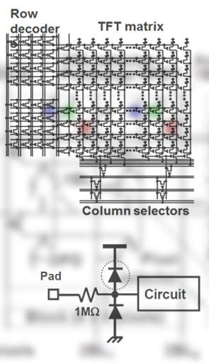
To realize the operation of large-scale integrated logic circuits, complementary metal oxide semiconductor (CMOS) inverters with a logic gate having a shape-reversal property (high gain) are indispensable. However, n-type organic semiconductors with a high mobility have a shallow lowest unoccupied molecular orbital (LUMO); therefore, they severely deteriorate and cannot exhibit a highelectrical property in atmosphere. We applied the pseudo-CMOS circuit, which is designed to realize the fabrication of inverters with an extremely high gain using only p-type semiconductors having a high mobility and stable performance in atmosphere, to organic transistors for the first time in the world, and succeeded in fabricating organic inverters that have a high gain and response speed while operating stably in atmosphere when driven at 2 V (IEEE Trans.Elec.Dev.2011, IEEE Elec.Dev.Lett. 2011). Thus, we have realized stable operation of large-scale integrated organic logic circuits.
Examples of large-scale integrated organic transistors include a sheet-type wireless power transmission system that can efficiently transmit at a high power of 70 Wviathe world’s first combination of plastic micro-electromechanical system (MEMS) switches and organic transistors (Nature Mater.2007), a prototype communication system (IEEE Trans.Elec.Dev.2009), and the world’s first large-area organic flash memory(Science2009).
A series of our achievements in developing large-scale integrated circuitshas been acceptedby the International Solid-State Circuits Conference (ISSCC), which is the highest-authority international conference in the field of electronic circuits and is called the Olympics of Electronic Circuits, for ten consecutive years. This record is still ongoing [e.g., IEEE J. Sol.State.Circuit2005, 2007, 2010, 2011, 2012, 2013]
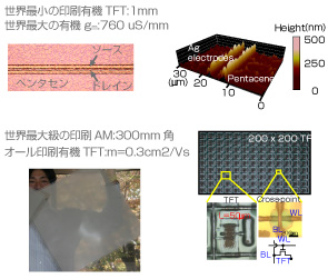
4 Improvement of performance of printed organic transistors and development of large-area electronics
Silicon technologyis one of the inorganic semiconductor technologiesthat support the current information communication technology (ITC), but fabrication of large-area silicon electronics is difficult. Focusing on this, we have been pioneering the work on large-area printing sensor systems for fabricating large-area electronics using organic materials (IEEE Trans.Elec.Dev.2010, Nature Mater. 2007, Appl.Phys.Lett. 2008, 2007, 2006). In particular, we were the first to succeed in applying ink-jet printing using attoliter droplets, which are one-thousandth the size of a droplet used in conventional ink-jet printing, to the fabrication of active devices (PNAS2008, MRS Comm. 2011). We realized the fabrication of the world’s smallest top-contact organic transistor(channel length, 1 μm) by this printing process, leading to the exploration of new processes in the field of printing electronics.
5 Development of ultraflexible and stretchable electronics
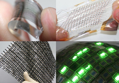
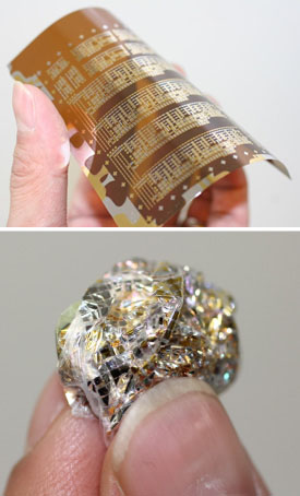
Since 2008, large-area organic electronics have been applied to devices used forobtaining human bioinformation. In particular, sensors to beattached tothe human skin should be conductive like metals and stretchable like rubber. On the basis of this idea, we developed rubber with the world’s highest conductivity using carbon nanotubes as an additive and succeeded in fabricating the first-ever large-area integrated circuit that is as stretchable as a rubber sheet. With this success, we have opened the door to a new field of stretchable electronics (Science2008, Nature Mater.2009, Adv.Mater.2010, MRSBulletin2012).
6 Development of imperceptible photonics
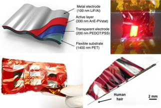
We have established a processingtechnology that can minimize the damage of substrate films as much as possible during the fabricationof semiconducting layer, electrode layer, and insulating layer of organic transistors by the self-assembly of organic materials. Applying this processing technology, we succeeded in fabricating a highly integrated circuit on a 1-μm-thick ultrathin film. We also realized the world’s thinnest and lightest organic electronic circuits (Nature2013), organic LEDs (Nature Photo.2013), and OPDs (Nature Comm.2012). We applied these devices to next-generation imperceptible electronics to be used in medicine andmedical welfare.
7 Development of Biopotential Sensors Using Flexible Devices
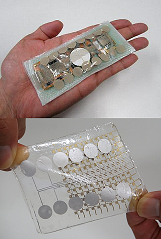
In this study, we developed an EEG sensor that achieves measurement accuracy comparable to that of large medical equipment by integrating highly conductive stretchable wiring, an ultra-high-precision analog front end, and low-power wireless technology.
Compared with conventional EEG systems that
require several meters of cabling, our sensor is only 6 mm thick and weighs 24 g, allowing users to simply attach it to the forehead for easy brain-wave measurement.
Using this EEG sensor, we demonstrated that it is possible to distinguish between patients with Alzheimer’s-type dementia and healthy individuals based solely on recorded brain activity.
Moving forward, we aim to enable simple dementia screening in home environments, local clinics, and nursing care facilities.