The Quantum Beam Materials Science Division studies chemical reactions and reaction fields, induced in materials by quantum beams under extreme conditions such as in the single-nanometer space region or in high-temperature, high-pressure and supercritical conditions, Using state-of-the-art quantum beams (electron beams, EUV, lasers, synchrotron radiation, X-rays, gamma rays, ion beams).
We are elucidating chemical reaction systems from the application of energy to materials by quantum beams, through chemical reactions to the discovery of functions, constructing new chemical reaction systems based on the knowledge obtained and it will be useful for the development of materials and processes.
In materials and process development, we conduct research and development of nanofabricated materials and processes for EUV lithography, which is used in the manufacture of cutting-edge semiconductor devices.
In order to achieve carbon neutrality, it is essential to reduce the power required for digital information processing, which will continue to increase exponentially in the future, and nanofabrication technology is a key technology for manufacturing high-performance devices.
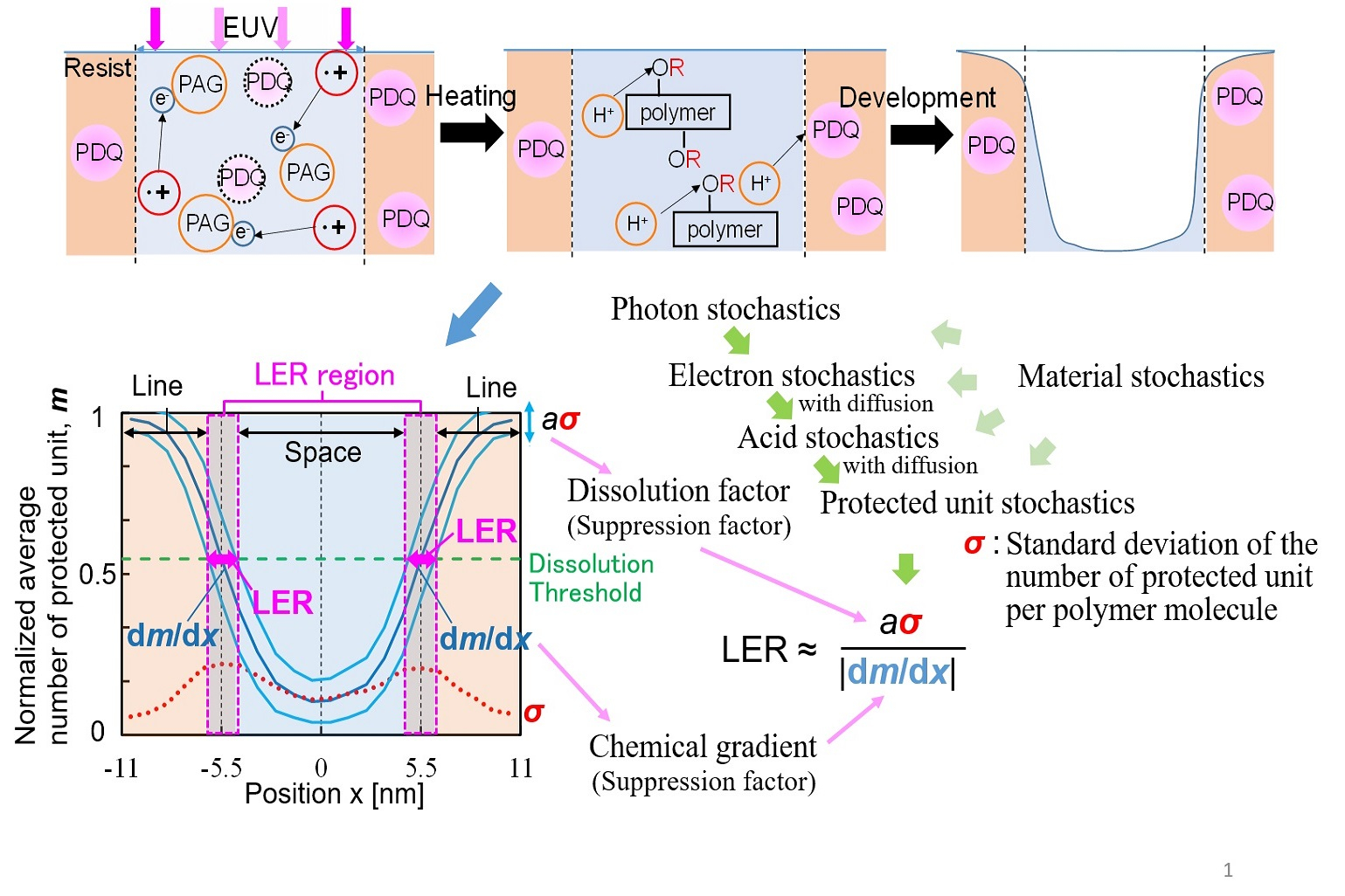
We have elucidated the mechanism of line width fluctuation called line edge roughness, which is a problem in state-of-the-art semiconductor lithography.
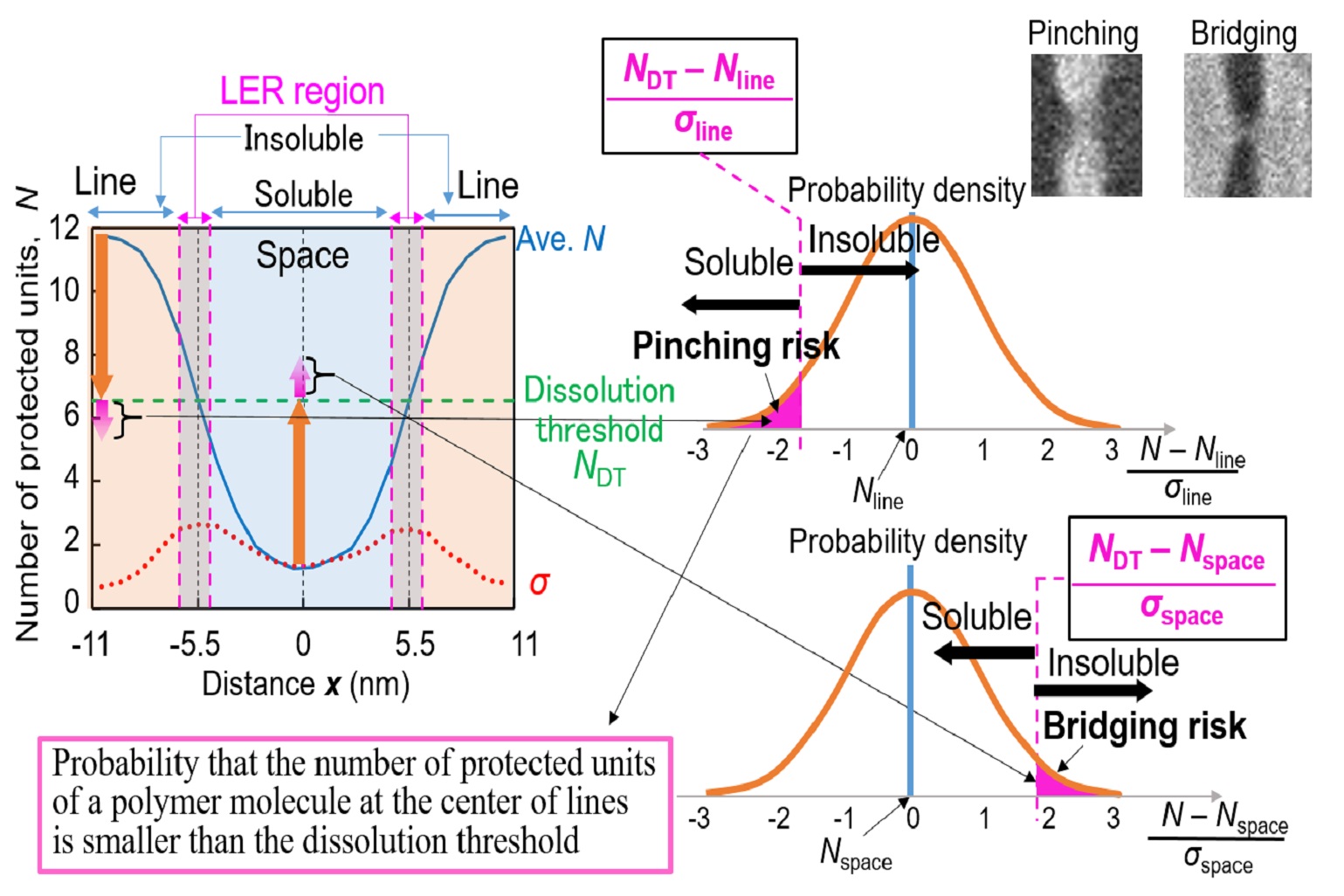
We have elucidated the generation mechanism of stockastic defects, which is the biggest challenge in the development of next-generation lithography.
Current Research Topics
Analysis of resist images with pattern defects by Hough transform Yuqing Jin, Takahiro Kozawa, Kota Aoki, Tomoya Nakamura, Yasushi Makihara, & Yasushi Yagi, Jpn.J.Appl.Phys.62, 086502(2023), DOI 10.35848/1347-4065/acea0c
Reaction mechanisms of Sn-complex-side-chain polymer used for extreme ultraviolet lithography, studied by electron pulse radiolysis and γ-radiolysis Yui Takata, Yusa Muroya, Takahiro Kozawa, Kohei Machida, Satoshi Enomoto, Bilal Naqvi, & Danilo De Simone, Jpn.J.Appl.Phys. 62, 076502 (2023), DOI:10.35848/1347-4065/ace012
Defect risks at interfaces of chemically amplified resists in extreme ultraviolet lithography process Takahiro Kozawa, Jpn.J.Appl.Phys. 62, 076501 (2023), DOI:10.35848/1347-4065/acde28
Dissolution dynamics of partially protected poly(4-hydroxystyrene) in tetraalkylammonium hydroxide aqueous solution Hitomi Betsumiya, Yuko Tsutsui Ito, Takahiro Kozawa, Kazuo Sakamoto, and Makoto Muramatsu, Jpn. J. Appl. Phys. 62, 036503 (2023), DOI:10.35848/1347-4065/acc222
Sensitization mechanism of metal oxide nanocluster resists with carboxylic acid ligands, Tomoe Otsuka, Yusa Muroya, Takuya Ikeda, Yoshitaka Komuro, Daisuke Kawana and Takahiro Kozawa,Jpn. J. Appl. Phys. 61, 086508 (2022), DOI:10.35848/1347-4065/ac7dd3.