

 Challenges of Nanochemistry in Mass Production of Semiconductors
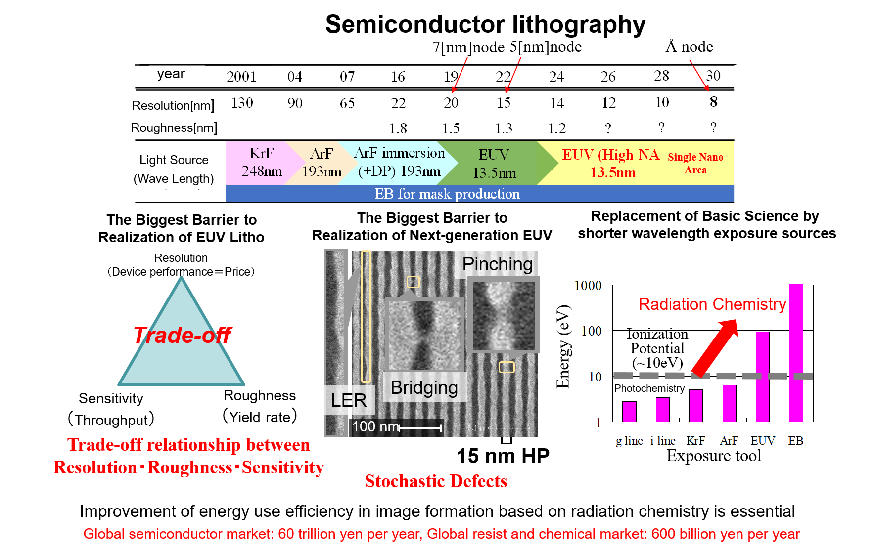
Today's semiconductor industry is supported by an ultrafine processing technology called lithography.
Lithography technology is advancing year by year, and by 2018, even mass production lines are processing lines with line widths of less than 20 nm.
In 2019, EUV light at 92.5 eV in the ionizing radiation regime will replace conventional light in the non-ionizing radiation regime as the next exposure source. EUV is expected to be in practical use from a resolution of 16 nm, called the N7 or 7 nm node, and to continue to be used in the sub-10 nm (single nano) resolution region, called the N2 or 2 nm node.
The realization of EUV lithography will be the first time that ionizing radiation is used in a major process for the mass production of semiconductors, and will mark a major development in the industrial use of quantum beams.
Quantum beams, which are in the ionizing radiation range, can impart energy to a finer area and cause chemical reactions than can be achieved using light because of their shorter wavelength. However, because the energy of the exposure source exceeds the ionization energy of common materials, this means a shift in material design from image formation using the excited state of photosensitive molecules to image formation using the ionization of the material matrix and secondary electrons, necessitating a drastic change in material design.
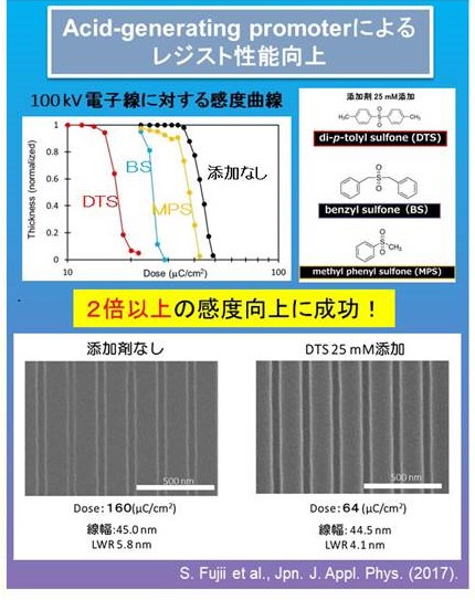
Furthermore, it is known that there is a trade-off relationship between resolution, sensitivity, and roughness, which are the main performance characteristics of photoresists, and this is a major obstacle to the development of new materials.
In order to solve the trade-off problem, it is essential to improve the efficiency of photon energy use in resist image formation.
To this end, elucidation of the phenomena induced by light in a space of a few nm and design of highly efficient reaction systems are essential for the development of new materials.
Extreme Ultraviolet Photochemistry of Condensed Phases
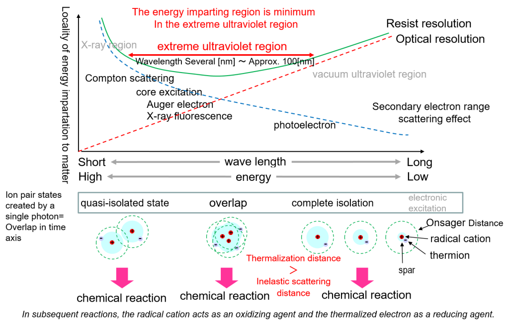
Radiation chemistry in the extreme ultraviolet region is not only an unexplored area, but also provides extreme spatial and time resolution for understanding radiation chemistry reactions.
In particular, the extreme ultraviolet region is an important energy region for elucidating the spatial distribution of cation-electron ion pairs produced as a result of the interaction of quantum beams with molecules and the details of subsequent chemical reactions.
Beam-induced Reaction Research Under Extreme Conditions
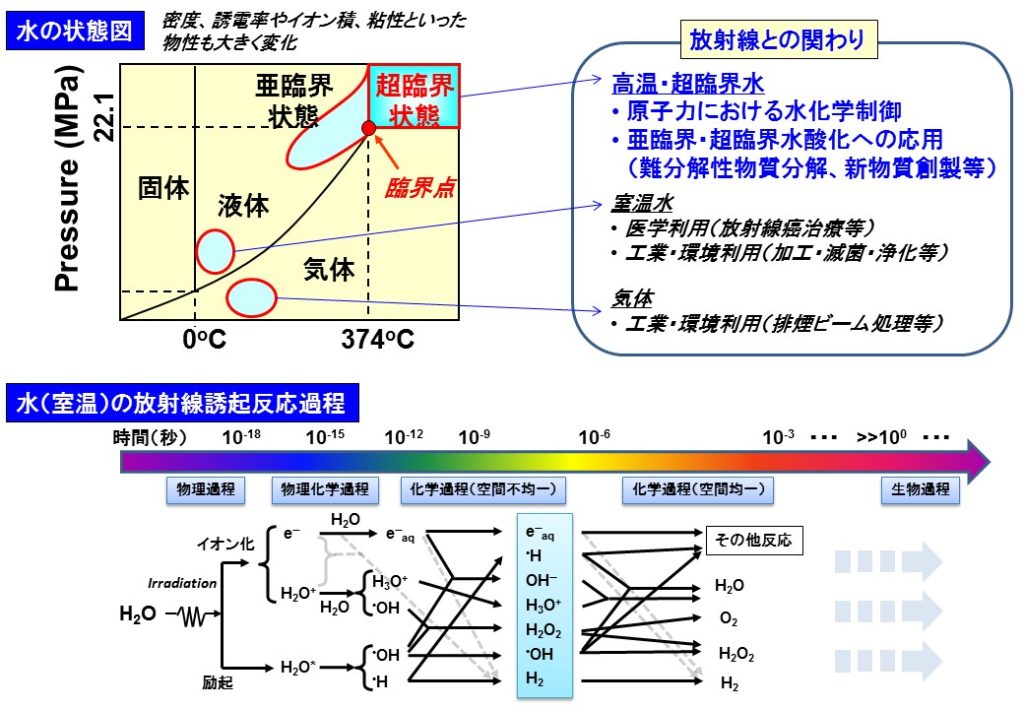
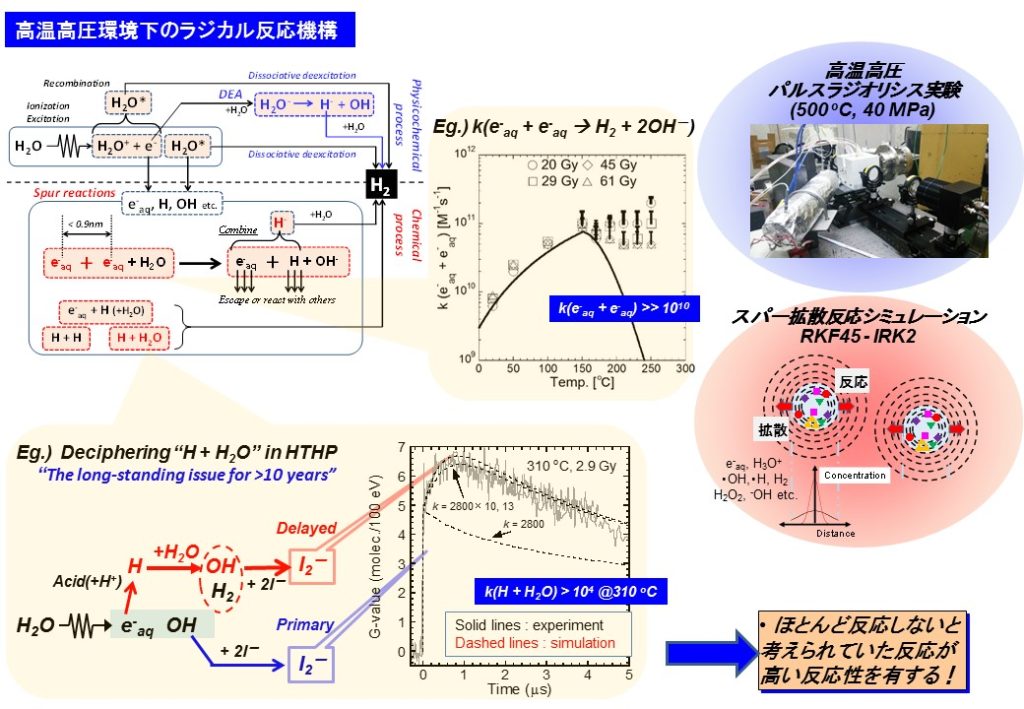
We will elucidate the interaction of materials under extreme conditions, such as high temperature, high pressure, and supercritical conditions, with radiation.
For example, water, under extreme conditions, changes its physical properties greatly depending on temperature and pressure, and at temperatures above 374oC and pressures above 22.1 MPa, it enters a supercritical state where the density also changes greatly depending on the pressure.
Although the reaction system induced by radiation is complex, parameters such as temperature, pressure, and density can be significantly changed in extreme conditions, and we investigate the essence of radiation-induced chemical reactions that cannot be distinguished at room temperature. We aim to understand and control these reactions in order to open up new fields such as the application of high-temperature and supercritical water to environmental science and the control of radiation effects in nuclear power generation.
State diagram of water and radiation-induced reaction processes in water (room temperature)
Ultrafast processes: energy imparting by beam irradiation and electron relaxation processes
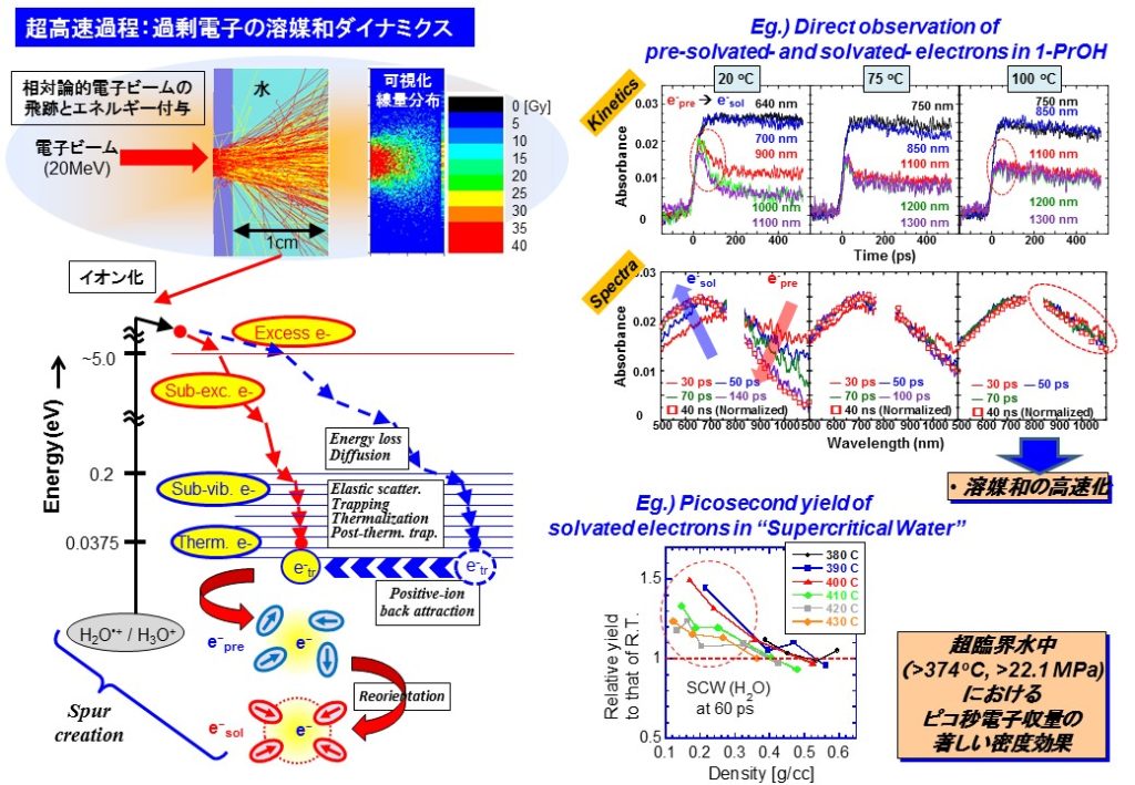
Nanospace reaction processes in polar solvents
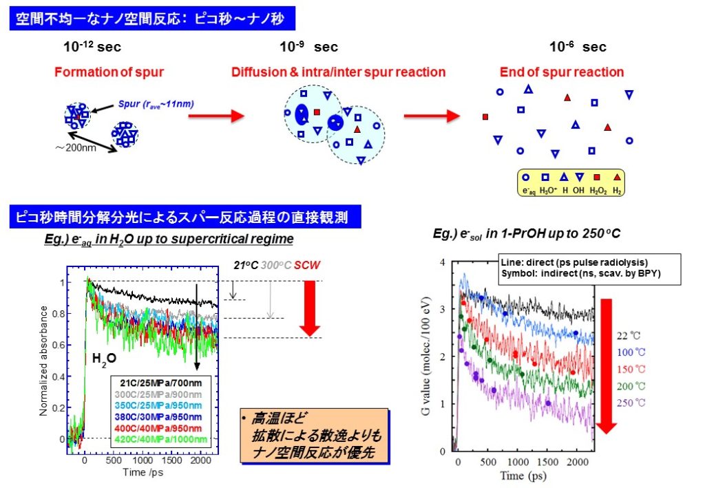
Radical Reaction Mechanisms in Subcritical to Supercritical Conditions
Radiation Chemistry Studies of Nanoparticles and Colloidal Solutions
Nanoparticles and colloids are attracting attention in various fields as novel functional materials with new catalytic activity and high durability.
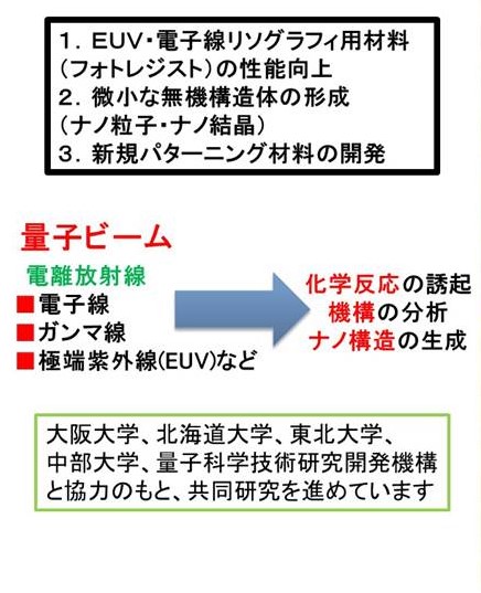
Quantum beams such as extreme ultraviolet (EUV) light, electron beams, and gamma rays are expected to be used in beam application engineering (next-generation lithography technology), nuclear engineering (light water reactor water chemistry), metal resists with high etching resistance (new resist materials), and noble metal colloids with high corrosion resistance (new injection materials for cooling water).
In addition to the elucidation of the fundamental process of nanoparticle formation induced by quantum beams and the interfacial reactions after formation, we aim to search for new reaction pathways and their reaction control.
Tracking the process of nanoparticle formation in platinum suspensions
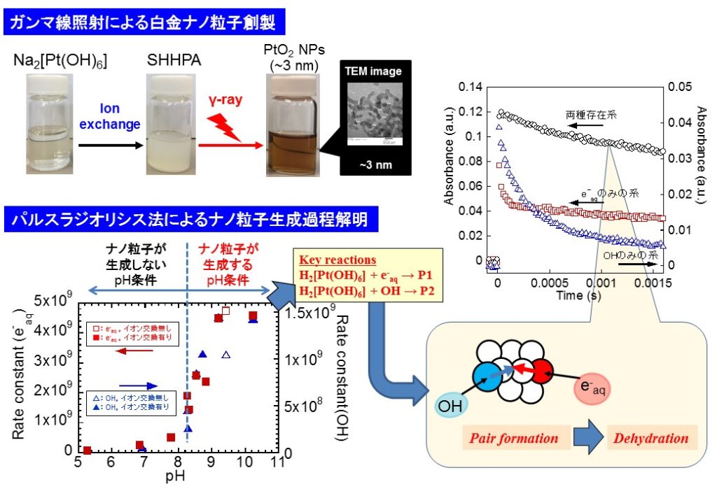
Initial Process of Quantum Beam-Induced Reaction of Nanoparticle Ligands
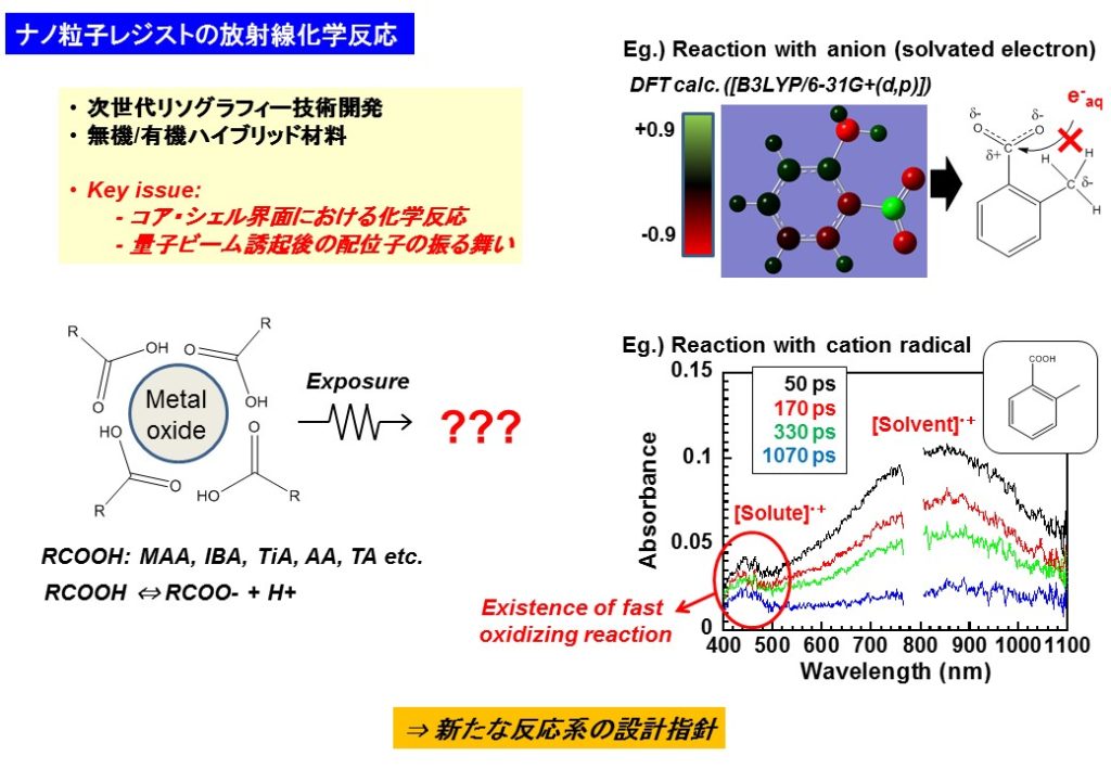
Quantum Beam-induced Organic and Inorganic Nanostructure Formation Mechanisms and Applications
Materials Design by Machine Learning
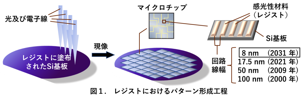
The performance of the photosensitive material called resist used in the lithography process determines the accuracy of semiconductor circuits (Figure 1).
The finer the circuit, the higher the circuit integration rate, the lower the power consumption, and the lighter and more powerful the device. Currently, research and development is underway to achieve a resolution of 8 nm (single nm) by 2031.
Low power consumption of semiconductors is essential to achieve carbon neutrality in response to future increases in information volume. The most important development element for achieving further miniaturization in the future is resist materials. However, as the line width of patterns becomes finer than before, the effects of pattern defects caused by stochastic chemical reactions during patterning become apparent and are a serious obstacle to miniaturization.
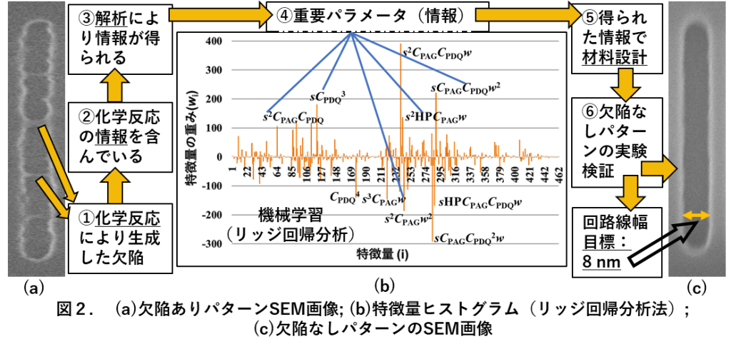
The information on chemical reactions is extracted from the nanoscale defect shape of a pattern with defects (Fig. 2(a)) (Fig. 2(b)), and the goal is to reduce the circuit line width to 8 nm without pattern defects by improving and creating a resist material (Fig. 2(c)).
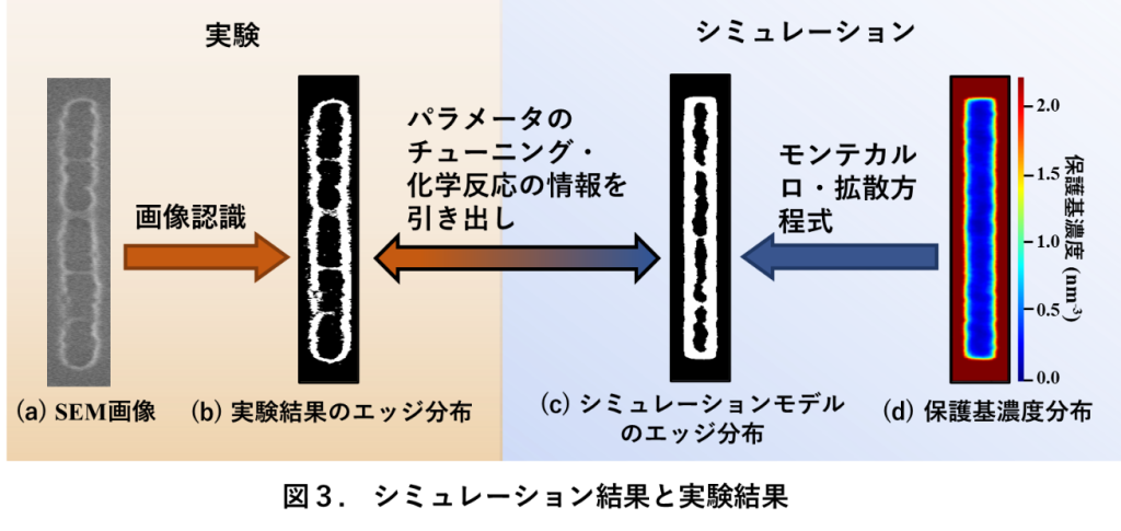
The research method involves first conducting experiments under different material compositions and process conditions and collecting data.
Information is extracted from the experimental results through automatic recognition of the pattern defect shape and analysis of the shape (Figures 3(a) and 3(b)). Next, model-based machine learning is performed by comparing the results with simulations. The simulation predicts the defect shape and is fitted to the obtained edge classes (Figures 3(c) and 3(d)), enabling the estimation of physical property values that cannot be obtained by ordinary measurement. Finally, the obtained information is used to synthesize resist materials and optimize process conditions.
Research on the Development Process
Coming Soon...
Metal Resist Research
Coming Soon...