Cellulose is a natural and easy to source material derived from wood. Cellulose nanofibers (nanocellulose) can be made into sheets of flexible nanocellulose paper (nanopaper) with dimensions like those of standard A4. Nanopaper does not conduct an electric current; however, heating can introduce conducting properties. Unfortunately, this exposure to heat can also disrupt the nanostructure.
The researchers have therefore devised a treatment process that allows them to heat the nanopaper without damaging the structures of the paper from the nanoscale up to the macroscale.
"An important property for the nanopaper semiconductor is tunability because this allows devices to be designed for specific applications," explains study author Hirotaka Koga. "We applied an iodine treatment that was very effective for protecting the nanostructure of the nanopaper. Combining this with spatially controlled drying meant that the pyrolysis treatment did not substantially alter the designed structures and the selected temperature could be used to control the electrical properties."
The researchers used origami (paper folding) and kirigami (paper cutting) techniques to provide playful examples of the flexibility of the nanopaper at the macrolevel. A bird and box were folded, shapes including an apple and snowflake were punched out, and more intricate structures were produced by laser cutting. This demonstrated the level of detail possible, as well as the lack of damage caused by the heat treatment.
Examples of successful applications showed nanopaper semiconductor sensors incorporated into wearable devices to detect exhaled moisture breaking through facemasks and moisture on the skin. The nanopaper semiconductor was also used as an electrode in a glucose biofuel cell and the energy generated lit a small bulb.
"The structure maintenance and tunability that we have been able to show is very encouraging for the translation of nanomaterials into practical devices," says Associate Professor Koga. "We believe that our approach will underpin the next steps in sustainable electronics made entirely from plant materials."
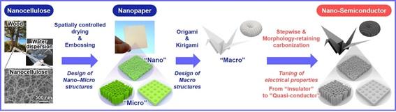
Fig.1 Schematic diagram of the preparation of the wood nanocellulose-derived nano-semiconductor with customizable electrical properties and 3D structures (cc BY, credit: 2022 Koga et al. Nanocellulose paper semiconductor with a 3D network structure and its nano−micro−macro trans-scale design. ACS Nano)
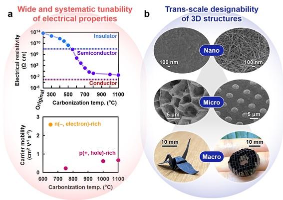
Fig.2 (a) Wide and systematic tunability of the electrical properties and (b) nano-micro-macro trans-scale designability of 3D structures of the as-prepared semiconductor (denoted the nanopaper semiconductor) (CC BY, credit: 2022 Koga et al. Nanocellulose paper semiconductor with a 3D network structure and its nano−micro−macro trans-scale design. ACS Nano)
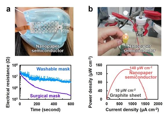
Fig.3 Device demonstrations using the nanopaper semiconductor. (a) Wearable sensor for monitoring human exhalation-derived water vapor leaked from facial masks. Washable mask: Sensor response pulses corresponding to respiration were observed, indicating a water vapor leak from the washable mask. Surgical mask: Only a gradual decrease in sensor resistance was observed, indicating the effective water vapor capture of the surgical mask. (b) Glucose biofuel cell for energy generation. The nanopaper semiconductor demonstrated a power density 14 times higher than that of a commercial graphite sheet, and led to illumination of a red LED. (CC BY, credit: 2022 Koga et al. Nanocellulose paper semiconductor with a 3D network structure and its nano−micro−macro trans-scale design. ACS Nano)
The article, "Nanocellulose paper semiconductor with a 3D network structure and its nano−micro−macro trans-scale design," was published in ACS Nano at DOI: https://doi.org/10.1021/acsnano.1c10728.


