Powering the future – ultrathin films are revolutionizing electrical conductivity


Researchers from SANKEN (The Institute of Scientific and Industrial Research), at Osaka University find a way to preserve the electrical properties of complex materials even at the nanoscale
Osaka, Japan – What if your electronic devices could adapt on the fly to temperature, pressure, or impact? Thanks to a new breakthrough in downsizing quantum materials, that idea is becoming a reality.
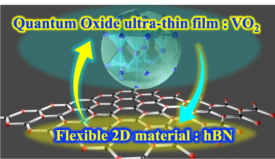
In an article published this month in Applied Physics Express, a multi-institutional research team led by Osaka University announced that they have successfully synthesized an ultrathin vanadium dioxide film on a flexible substrate, in a way that preserves the film’s electrical properties.
Vanadium dioxide is well known in the scientific community for its ability to transition between conductor and insulator phases at nearly room temperature. This phase transition underpins smart and adaptable electronics that can adjust to their environment in real time. But there is a limit to how thin vanadium dioxide films can be, because making a material too small affects its ability to conduct or insulate electricity.
“Ordinarily, when a film is placed on a hard substrate, strong surface forces interfere with the atomic structure of the film and degrade its conductive properties,” explains Boyuan Yu, lead author of the study.
To overcome this limitation, the team prepared their films on two-dimensional hexagonal boron nitride (hBN) crystals; hBN is a highly stable soft material that does not have strong bonds with oxides and thus does not excessively strain the film or spoil its delicate structure.
“The results are truly surprising,” says Hidekazu Tanaka, senior author. “We find that by using this soft substrate, the material structure is very nearly unaffected.”
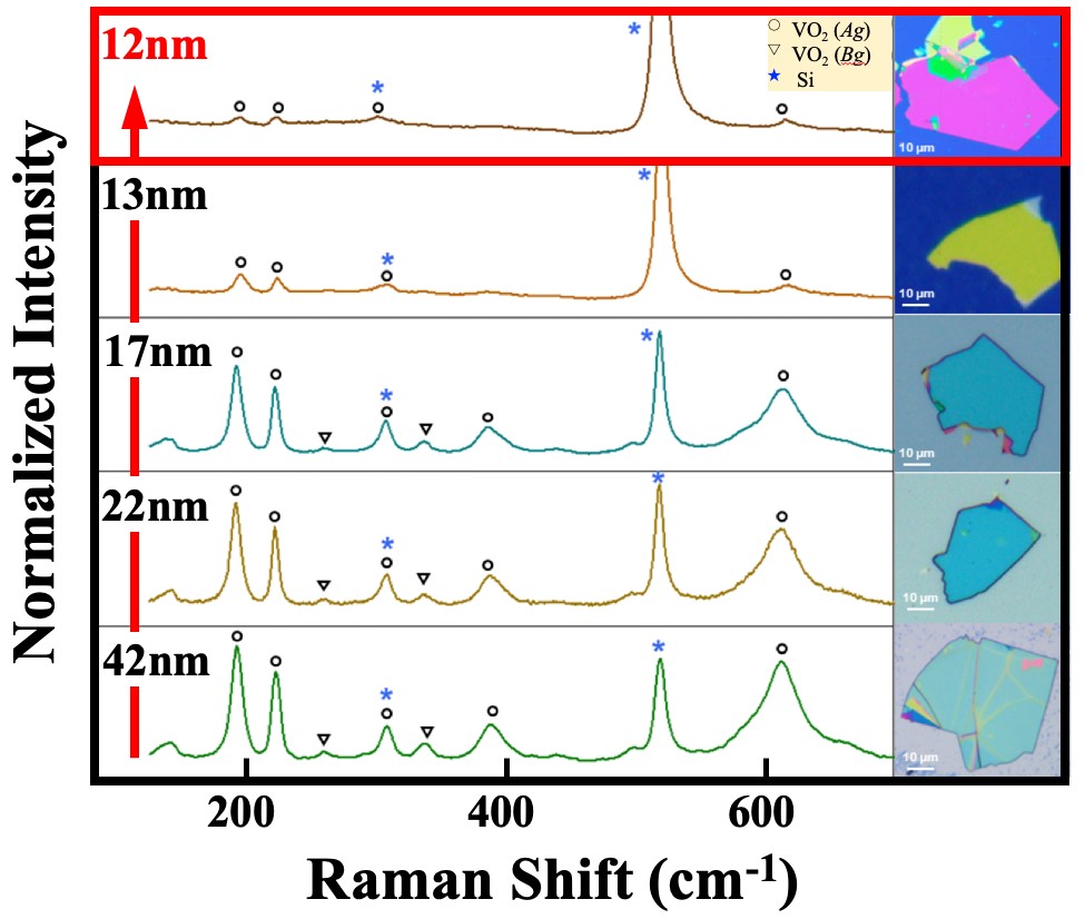
By performing precise spectroscopy measurements, the team was able to confirm that the phase transition temperature of their vanadium dioxide layers remained essentially unchanged, even at thicknesses as thin as 12 nm.
“This discovery significantly improves our ability to manipulate quantum materials in practical ways,” says Yu. “We have gained a new level of control over the transition process, which means we can now tailor these materials to specific applications like sensors and flexible electronics.”
Given that quantum materials like vanadium dioxide play a crucial role in the design of microsensors and devices, this discovery could pave the way for functional and adaptable electronics that can be attached anywhere. The research team is currently working on such devices, as well as exploring ways to incorporate even thinner films and substrates.
###
The article, “Strain-free thin film growth of vanadium dioxide deposited on 2D atomic layered material of hexagonal boron nitride investigated by their thickness dependence of insulator–metal transition behavior,” was published in Applied Physics Express at DOI: https://doi.org/10.35848/1882-0786/adaf09
Summary
A multi-institutional research team led by Osaka University has engineered a way to preserve the electrical properties of materials as they are shrunk to the nanoscale. The use of the soft substrate hexagonal boron nitride reduces damage to the atomic structure caused by strain, allowing materials to keep their conductive properties as films as thin as 12 nm.A multi-institutional research team led by Osaka University has engineered a way to preserve the electrical properties of materials as they are shrunk to the nanoscale. The use of the soft substrate hexagonal boron nitride reduces damage to the atomic structure caused by strain, allowing materials to keep their conductive properties as films as thin as 12 nm.
Keywords
Materials science
Electrical properties,
metal oxides,
electrical conductivity,
thin films,
nanomaterials,
quantum phase transitions,
nanocrystals,
transition metal oxides,
optoelectronics