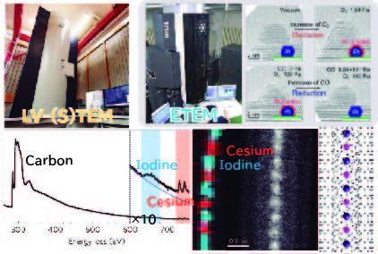
State-of-the-art electron microscopy (upper left), single-atom elemental map for CsI (lower), oxidation-reduction reaction of Pt nanoparticle (upper right)
Recently, material science research has intensified in an attempt to understand materials at the atomic level and apply them to electronic devices or battery materials. We perform the front-line material research by using the cutting-edge electron microscopy techniques. We develop low-voltage TEM/STEM which enables the single molecular imaging and single atom spectroscopy, and high-resolution environmental TEM for the in situ observations of interaction of solid surface with gas atmosphere to realize novel nanostructures and unforeseen properties.
| 2021- | Distinguished professor, Osaka University |
| 2001-2021 | AIST (National Institute of Advanced Industrial Sci and Tech.) |
| 1998-2001 | JST Nanotubulites project |
| 1997-1998 | Solid state physics lab, Univerisite Paris-Sud |
| 1994-1996 | Ecole nationale superieure des mines de Paris (Alan Thorel) |


Studies of atoms/molecules confined in nano-space
High resolution EELS for infra-red spectroscopy at a nanometer-scale
Momentum-resolved EELS in TEM
Synthesis of novel materials in an electronically stimulated nanogap
Atomic-scale structural analysis of nanodevices under working environment